Welcome to the Electronics Hardware Design section of Cadiora. Here you’ll find comprehensive guides, best practices, and practical tips for PCB design, schematic verification, and hardware development. Our content is designed to help both beginners and experienced engineers create reliable and efficient electronic designs.
Key Topics Covered
- PCB Design Guidelines: Learn essential practices for creating reliable and manufacturable PCBs
- EMC Compliance: Understand how to design boards that meet electromagnetic compatibility requirements
- Power Integrity: Master techniques for ensuring stable power delivery in your designs
- Component Placement: Discover strategies for optimal component arrangement
- Board Bring-Up: Follow systematic procedures for testing and validating new designs
- Design Verification: Use comprehensive checklists to ensure error-free designs
Design Resources
Our articles provide practical, hands-on guidance for electronics hardware design. Each guide includes:
- Detailed explanations of key concepts
- Step-by-step procedures
- Best practices and common pitfalls
- Real-world examples and case studies
- Comprehensive checklists and verification methods
Start exploring our content through the cards above to improve your electronics design skills and create more reliable hardware.
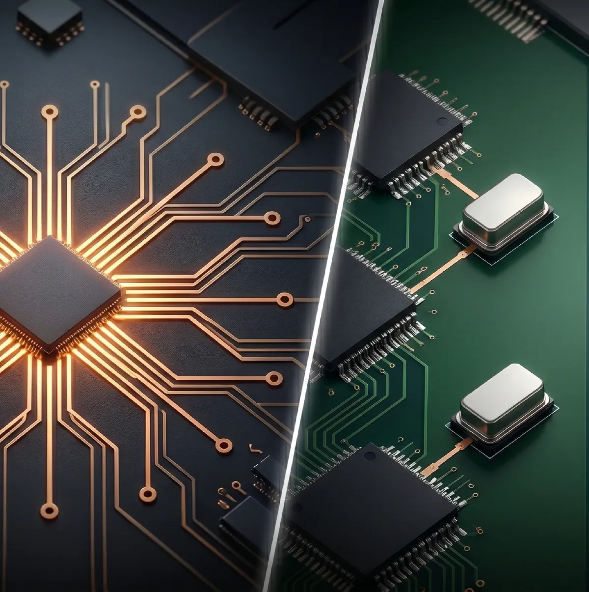
Centralized Clocking in FPGA/SoC Hardware Design: An Exercise in Optimization or a Single Point of Failure?
Comparative analysis of centralized clock hubs vs. distributed timing networks in FPGA/SoC designs—evaluating … Continue reading
Decoupling - Path to power integrity
Decoupling strategies for power integrity covering transient current suppression and multi-frequency design. Continue reading
Engineered to Doom - Red Flags for PCB Design
Identify critical PCB design mistakes: clock selection, signal routing, and grounding pitfalls. Continue reading
Strategy for component placement
PCB component placement strategies considering mechanical, manufacturing, and circuit design constraints. Continue reading
Selecting a PCB stack-up for EMC compliance
EMC-optimized PCB stack-up selection considering signal routing, frequency, and emission requirements. Continue reading
15 PCB Layout guidelines to achieve EMC requirements
EMC compliance guidelines for PCB layout covering signal integrity, grounding, and radiation management. Continue reading
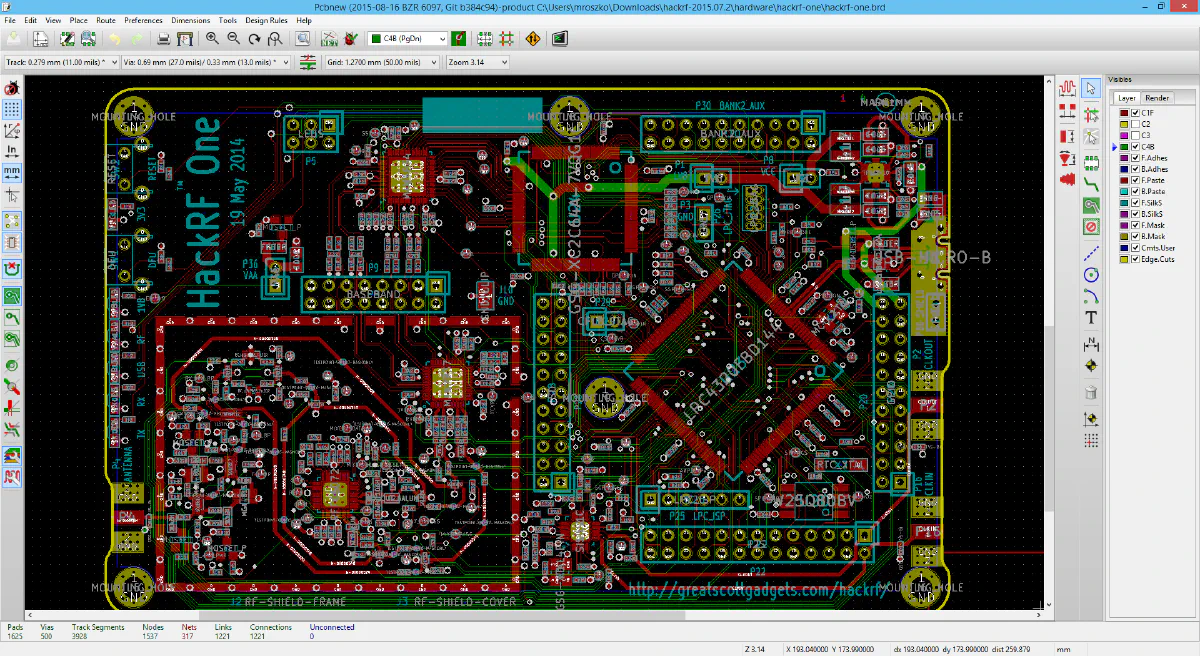
Checklist for error-free optimized PCB layout
Comprehensive PCB layout checklist covering footprints, placement, routing, and verification steps. Continue reading
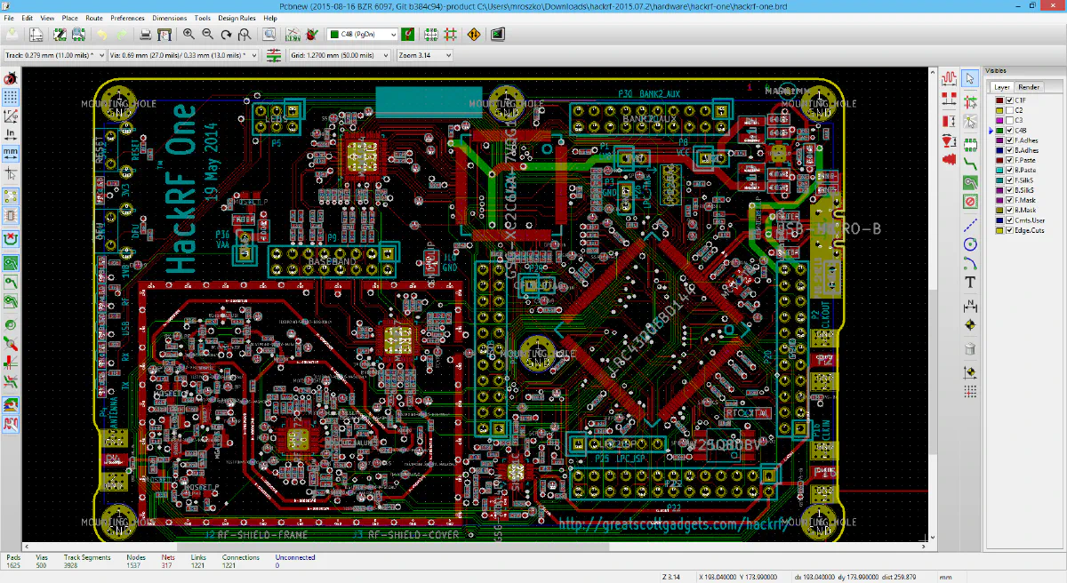
4 Steps to Review the PCB Layout
A comprehensive PCB layout review process covering data collection, placement verification, routing analysis, and … Continue reading

Board bring up: Giving life to the design
Complete board bring-up process covering assembly verification, testing, debugging, and validation steps. Continue reading
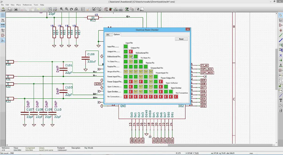
100 Point Checklist for Schematic Design
Comprehensive 100-point schematic design checklist covering design rules, components, and verification steps. Continue reading