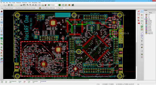
Checklist for error-free optimized PCB layout
Comprehensive PCB layout checklist covering footprints, placement, routing, and verification steps. Continue reading
Showing all posts with tag "Checklist"
Comprehensive PCB layout checklist covering footprints, placement, routing, and verification steps. Continue reading
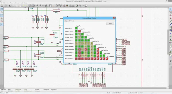
Comprehensive 100-point schematic design checklist covering design rules, components, and verification steps. Continue reading