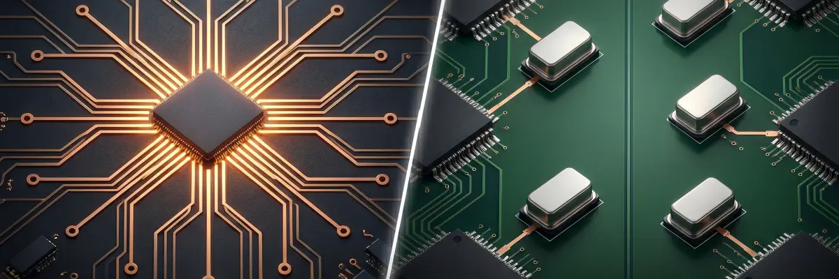
The clocking topology of modern Field Programmable Gate Arrays (FPGAs) and System-on-Chips (SoCs) dictates their operational performance, power envelope, and ultimate system reliability. As devices scale to integrate multi-gigabit transceivers, hard processor systems (HPS), and high-speed programmable fabric—exemplified by platforms such as the AMD (Xilinx) FPGA, Altera (Intel) Agilex 5/7/9, and Lattice Avant-G/CertusPro-NX—the timing distribution network becomes a battleground for competing architectural paradigms.
This article provides a comparative research analysis of the two dominant methodologies:
- The Centralized Clock Hub (utilizing a single-chip, multi-output fractional synthesizer like the Skyworks Si5332) versus
- The Distributed Timing Network (utilizing multiple, discrete fixed-frequency crystal oscillators).
We analyze these paradigms across reliability, spectral purity, signal routing, specialized phase-tracking applications (e.g., White Rabbit), and critical clock-domain crossing (CDC) guardrails.
Introduction: Internal PLLs vs. External References
Modern heterogeneous SoCs contain distinct, isolated silicon regions which are highly dense and with specific clocking needs.
Multi-Gigabit Transceivers (MGTs): Require ultra-low jitter reference clocks (e.g., 156.25 MHz, 312.5 MHz) to keep Bit Error Rates (BER) within strict telecom standards.
Processing Systems (PS): Demand low-frequency, stable references (e.g., 25 MHz, 33.33 MHz) to drive ARM processing cores and system peripherals.
Programmable Logic (PL): Runs fabric pipelines anywhere from 100 MHz to 500 MHz, depending on timing closure parameters.
GPU and NPU: Accelerator blocks demand independent, high-frequency clocks (often 400 MHz to 1+ GHz) with tight phase alignment to memory controllers.
To operate these domains, engineers frequently face a choice: leverage the on-chip Phase-Locked Loops (PLLs) and Mixed-Mode Clock Managers (MMCMs) to generate all required frequencies internally, or supply multiple discrete external reference clocks. While generating dozens of clocks internally from a single external reference is highly cost-effective, on-chip PLLs operate in highly volatile electrical environments. The digital fabric of SoC exhibits high-frequency switching noise, which couples directly into the internal clock distribution networks. This dynamic load causes power supply voltage fluctuations, degrading the jitter and phase noise performance of internal PLLs.
To achieve the spectral purity required for high-performance transceiver loops or ultra-low-jitter data converters, external clock generation remains superior. This necessity brings us to the core dilemma: do we generate these external clocks from a centralized multi-output device, or distribute the generation across physically isolated, discrete oscillators?
Spectral Purity: The Reality of Modern Drivers vs. Physical Air Gaps
Modern multi-output clock generators (such as the Skyworks Si5332) are marvels of silicon engineering. Featuring advanced internal low-dropout (LDO) regulators, isolated output buffer banks, and proprietary fractional divider technology, these chips can generate highly clean, independent frequencies with sub-picosecond RMS jitter.However, in the physical domain, nothing beats physical isolation.
graph LR
    subgraph Centralized ["Centralized Multi-Output Die (Crosstalk Risk)"]
        REF_C["Reference Crystal"] --> Div[MultiSynth Fractional Dividers]

        Div --> BankA["Bank A: 100.00 MHz"]
        Div --> BankB["Bank B: 156.25 MHz"]
        Div --> BankC["Bank C: 33.33 MHz"]

        BankA --> ETH_C["PCIe Subsystem"]
        BankB --> MGT_C["Gigabit Transceivers"]
        BankC --> PS_C["Processing System Clock"]
    end

    subgraph Distributed ["Distributed Network (Total Physical Isolation)"]
        XtalA["Discrete Crystal A
Isolated 100.00 MHz"] --> ETH_D["PCIe Subsystem"]
        XtalB["Discrete Crystal B
Isolated 156.25 MHz"] --> MGT_D["Gigabit Transceivers"]
        XtalC["Discrete Crystal C
Isolated 33.33 MHz"] --> PS_D["Processing System Clock"]
    end

    style Centralized fill:#fdf2f2,stroke:#f8b4b4,stroke-width:2px
    style Distributed fill:#f0fdf4,stroke:#bbf7d0,stroke-width:2px
When a single silicon die synthesizes multiple, non-integer-related frequencies (such as $100\text{ MHz}$ for PCIe, $125\text{ MHz}$ for Gigabit Ethernet, and $156.25\text{ MHz}$ for transceivers), high-frequency intermodulation products ($f_1 \pm f_2$) propagate through the shared silicon substrate. Even with excellent decoupling, switching noise from one output driver can modulate the phase of an adjacent clock channel.As a hardware designer, you must evaluate how much purity is actually required:
- High-Purity Constraints: If your board includes precision RF analog-to-digital converters (ADCs), high-resolution digital-to-analog converters (DACs), or sensitive Time-to-Digital Converters (TDCs), the spectral spurs introduced by a centralized chip can degrade system performance. These sections demand physically isolated, point-of-load oscillators.
- Standard Logic Constraints: For digital fabric, general-purpose processing systems, and standard communications interfaces (e.g., PCIe Gen4, GbE), the performance of a modern centralized clock generator is more than sufficient, making its density benefits highly attractive.
Reliability and Fault Containment
In high-reliability engineering, the choice between centralized and distributed architectures is a trade-off between system complexity and fault propagation.
The Centralized Clock Hub
In a centralized model, the clock generator chip represents a critical Single Point of Failure (SPOF). A localized power supply glitch, thermal overload, or clock chip crash instantly halts the entire system. Because all output buffers are derived from the same device, any internal failure cascades across the processing system (PS) and programmable logic (PL) simultaneously.
The Distributed Timing Network & The PS-PL Failure Caution
A distributed network eliminates the centralized SPOF, ensuring that a failing oscillator only takes down its localized subsystem. However, this introduces a crucial requirement for the designer: the programmable logic must be architected to handle subsystem failures gracefully.
If the processing system (PS) oscillator fails, the programmable logic (PL) fabric—running on its own independent clock—must not enter a hung or non-deterministic state. Designers must implement:
- Clock Loss Detection: Utilizing FPGA clock monitors or window watchdogs to detect when a reference clock stops toggling.
- Robust Handshaking: Implementing defensive state machines with timeout counters at all PS-PL boundaries. If the PS clock halts mid-transaction, the PL must gracefully abort the bus cycle, log the fault, and transition to a safe state rather than hanging indefinitely.
Specialized Applications: Phase Tuning and the “White Rabbit” Risk
In specialized networks requiring sub-nanosecond synchronization over Ethernet—such as the White Rabbit protocol or distributed Digitally Controlled Oscillator (DCO) setups—precision phase adjustment is mandatory. These applications highlight a severe risk inherent to centralized clocking.
graph LR
    subgraph Centralized_Crisis ["CENTRALIZED UPDATE CRISIS"]
        PLL[Centralized PLL / Core VCO] -->|VCO Phase Step Update| Out1[Output 1: Adjusting Phase]
        PLL -->|Core Frequency Shift Impact| Out2["Output 2: Loses Lock (LOL)"]
        PLL -->|Core Frequency Shift Impact| Out3["Output 3: Loses Lock (LOL)"]
        Out2 --> Fail[System-wide Failure / Sub-system Crashes]
        Out3 --> Fail
    end

    subgraph Distributed_Isolation ["DISTRIBUTED UPDATE ISOLATION"]
        DAC[DAC / Control Logic] -->|V_tune Voltage Modulation| VCXO[Isolated VCXO]
        VCXO -->|Clean Phase Shift| Target[Target Synchronized Domain]
        Other[Other Isolated Oscillators] -->|No Voltage Change| Safe[Other Clocks: Completely Stable]
    end

    style Centralized_Crisis fill:#fff5f5,stroke:#feb2b2,stroke-width:1px
    style Distributed_Isolation fill:#f0fdf4,stroke:#bbf7d0,stroke-width:1px
    style Out2 fill:#fee2e2,stroke:#ef4444
    style Out3 fill:#fee2e2,stroke:#ef4444
    style Safe fill:#dcfce7,stroke:#22c55e
When a system requires active phase or frequency steering, the clock reference must be continuously adjusted. In a distributed network using individual Voltage-Controlled Crystal Oscillators (VCXOs), tuning voltage or digital control is applied exclusively to the targeted clock. The adjustment is completely isolated and has zero impact on neighboring clock domains.
Conversely, if a centralized multi-output PLL is used, making a phase adjustment that exceeds the fractional divider’s seamless tracking window requires updating the core PLL or VCO feedback loop parameters. Re-locking or shifting the core PLL temporarily disrupts all output channels derived from that VCO. A phase update meant for a single synchronization interface can cause a momentary loss of lock (LOL) across all other system clocks, triggering a catastrophic system-wide reset.
The Clock Domain Crossing (CDC) Guardrail
A dangerous misconception exists among some system designers: “If all my logic blocks are driven by the same physical external clock source or frequency, I do not need Clock Domain Crossing (CDC) circuitry.” This assumption is false and introduces high-risk metastability bugs into your silicon.
graph TD
    Gen[Single External Clock Generator e.g., 100 MHz] -->|Clock Trace A| PS_PLL[PS Bank PLL]
    Gen -->|Clock Trace B| PL_PLL[PL Bank PLL]

    PS_PLL -->|Internal Net| PS_Clk[Processor Clock: Phase Drifts]
    PL_PLL -->|Internal Net| PL_Clk[Fabric Clock: Phase Drifts]

    PS_Clk -->|Data Path| Crossing{{"PS-PL Boundary(CDC Strictly Required)"}}
    PL_Clk -->|Data Path| Crossing

    style Crossing fill:#fef08a,stroke:#eab308,stroke-width:2px,color:#854d0e
Even if two digital domains (such as the Processing System and the Programmable Logic fabric) are supplied with the exact same external frequency:
- Independent Internal PLLs: The PS and PL process these signals through distinct, physically separated internal clock networks and hard PLL/MMCM blocks.
- Phase Drift and Jitter: Thermal variations, routing delays, and independent phase-noise characteristics cause the phase relationship between these internal clocks to drift dynamically over time.
Because the phase relationship between the two resulting clocks is non-deterministic, signals traversing the PS-PL boundary will inevitably violate setup and hold times at the destination flip-flops. Clock Domain Crossing (CDC) design practices (e.g., synchronizers, async FIFOs, handshaking) remain strictly mandatory, regardless of whether a single external clock chip is used.
System-Level Scope: FPGA SoC to Application Processors
This architectural trade-off is not unique to FPGAs. Modern highly integrated Application Processors, Multicore SoCs, and Automotive ASICs face the exact same clocking dilemma.
In automotive safety-critical designs (e.g., ADAS processors), distributing independent, isolated clocks to the safety island (the lockstep cores) and the high-performance neural processing units (NPUs) is standard practice. This physical isolation prevents a clock failure or localized noise glitch in the power-hungry consumer-facing logic from crashing the vehicle’s critical safety-control systems.
Comparative Architecture Matrix
| Architectural Parameter | Centralized Clock Hub (Single-Chip / Si5332) | Distributed Timing Network (Multiple Discrete XOs/VCXOs) |
|---|---|---|
| Systemic Reliability | Poor (SPOF): Single IC failure causes immediate, total system collapse. | Excellent: Faults are contained locally; allows for graceful system degradation. |
| Phase Noise & Spurs | Moderate: 0.3-0.8 ps RMS jitter; -125 dBc/Hz @ 100 Hz offset. | Superior: 0.15-0.4 ps RMS jitter (VCXO); -145 to -160 dBc/Hz @ 100 Hz offset. |
| Active Phase Steering | High Risk: Core VCO adjustment can break lock on unrelated output channels. | Safe & Isolated: Adjusting a single VCXO has zero impact on surrounding domains. |
| BOM Cost (4-6 clocks) | $8.50 - $15.00 (single chip) | $7.20 - $48.00 (depending on precision grade) |
| Power Consumption | 180 - 320 mW (shared PLL core, scales moderately) | Configuration-dependent: 120-300 mW (6× standard); 300-900 mW (6× VCXO/TCXO) |
| PCB Routing Complexity | High: Congested star topology with critical impedance control. | Low: Point-of-load placement; short, isolated traces. |
| CDC Requirement | Strictly Mandatory: Separate internal PLLs make clock crossings non-deterministic. | Strictly Mandatory: No phase relationship exists between independent sources. |
| Hardware Flexibility | Excellent: Software-defined NVM profiles allow on-the-fly frequency/phase tuning. | None: Rigid; modification requires physical component desoldering. |
| Best Use Case | Cost-sensitive, flexible designs; moderate jitter tolerance; rapid prototyping. | Ultra-low jitter systems; precision analog front-ends; safety-critical fault isolation. |
Conclusion: The Architectural Verdict
Ultimately, declaring one clocking methodology superior to the other ignores the nuances of practical system architecture. The choice between a centralized hub and a distributed timing network is a deliberate exercise in engineering optimization.
Select a Centralized Clock Hub when:
- Design requires 4+ different clock frequencies (power efficiency advantage)
- Post-production frequency flexibility is critical
- BOM cost must be minimized (<$15 for entire clock distribution)
- RMS jitter <1 ps is acceptable for your application
- Rapid prototyping with software-defined clocking is needed
- Consistent thermal profile preferred over distributed heat sources
Enforce a Distributed Timing Network when:
- Absolute fault isolation is mandatory (safety-critical, ASIL-D automotive)
- Phase noise floor <-150 dBc/Hz @ 10 kHz is required (precision ADC/DAC ≥16-bit)
- Active phase steering is needed (White Rabbit, DCO synchronization)
- Point-of-load placement reduces routing congestion
- Only 2-3 clock frequencies needed (potential power advantage with standard oscillators)
- Thermal isolation from analog circuitry is critical (avoid localized hotspot)
Consider a Hybrid Approach when:
- Sensitive analog/RF sections demand isolated VCXOs
- Digital logic and standard interfaces benefit from centralized flexibility
- Cost and performance must be balanced across subsystems
As FPGA and SoC platforms continue to integrate higher-speed transceivers and denser logic fabric, the clocking architecture decision becomes increasingly consequential. Armed with quantitative metrics, a systematic decision framework, and authoritative industry references, hardware engineers can confidently architect timing distribution networks optimized for their application’s unique performance, reliability, and cost constraints.
Quantitative Performance Metrics
To make informed architectural decisions, engineers require concrete performance data rather than qualitative assessments. The following quantitative comparison provides measurable benchmarks for real-world design trade-offs.
Cost Analysis
| Component Type | Unit Cost (USD, 2026) | Typical Configuration | Total BOM Cost |
|---|---|---|---|
| Centralized Clock Hub (e.g., Si5332, Si5341) | $8.50 - $15.00 | 1 chip, 4-12 outputs | $8.50 - $15.00 |
| Discrete Oscillators (Standard CMOS) | $1.80 - $3.50 | 4-6 independent oscillators | $7.20 - $21.00 |
| High-Precision VCXO/TCXO | $4.50 - $12.00 | 3-4 precision oscillators | $13.50 - $48.00 |
Design Insight: For cost-sensitive, high-volume consumer products, a centralized solution provides excellent value. For ultra-low-jitter RF/analog applications requiring VCXOs, the distributed network’s BOM cost increases significantly but delivers superior spectral performance.
Power Consumption
| Architecture | Typical Power (mW) | Notes |
|---|---|---|
| Centralized Hub (Si5332, 4 outputs active) | 180 - 250 mW | Single shared VCO/PLL core; scales moderately with active outputs |
| Centralized Hub (Si5332, 8 outputs active) | 250 - 320 mW | Higher output count increases buffer power |
| Distributed Network (4× standard CMOS oscillators) | 80 - 200 mW (total) | 20-50 mW per discrete oscillator |
| Distributed Network (6× standard oscillators) | 120 - 300 mW (total) | Power scales linearly with oscillator count |
| High-Performance VCXO (per unit) | 50 - 150 mW | Temperature-compensated (TCXO): 30-80 mW |
| Oven-Controlled Crystal (OCXO) (per unit) | 1000 - 3000 mW | Maintains oven at constant temperature |
Design Insight: Power comparison is configuration-dependent:
- Centralized wins when 5+ clocks are needed: shared PLL core is more efficient than multiple discrete oscillators
- Distributed wins when only 2-3 low-power clocks are required: avoids overhead of full clock synthesizer
- Distributed loses significantly when high-precision VCXOs or OCXOs are required: a single OCXO can consume more power than an entire centralized hub
- Thermal consideration: Centralized hubs create a single 250-320 mW hotspot; distributed networks spread heat across the PCB, beneficial for thermally-sensitive analog circuitry in close proximity
Jitter and Phase Noise Performance
| Parameter | Centralized Hub (Si5332) | Discrete Crystal Oscillator | High-End VCXO |
|---|---|---|---|
| RMS Jitter (12 kHz - 20 MHz) | 0.3 - 0.8 ps | 0.5 - 1.2 ps | 0.15 - 0.4 ps |
| Phase Noise @ 100 Hz offset | -115 to -125 dBc/Hz | -130 to -145 dBc/Hz | -140 to -160 dBc/Hz |
| Phase Noise @ 10 kHz offset | -135 to -145 dBc/Hz | -150 to -160 dBc/Hz | -160 to -170 dBc/Hz |
| Typical Application | PCIe Gen4/5, 10GbE, DDR5 | General FPGA clocking, GbE | Precision ADC/DAC (≥16-bit), RF transceivers |
Critical Thresholds:
- 10 Gigabit Ethernet (10GBASE-R): Requires <1 ps RMS jitter to maintain BER < $10^{-12}$
- PCIe Gen5 (32 GT/s): Demands <0.5 ps RMS jitter for reliable link training
- 16-bit+ ADC/DAC: Phase noise floor below -155 dBc/Hz @ 10 kHz offset to avoid SNR degradation
PCB Area and Routing Complexity
| Metric | Centralized | Distributed |
|---|---|---|
| Clock IC Footprint | 16-24 mm² (single QFN/TQFP) | 12-40 mm² total (4-6 × 3×2.5 mm oscillators) |
| Decoupling Network | Compact: localized 3-5 capacitors | Distributed: 2-3 caps per oscillator across board |
| Trace Routing Complexity | High: Star topology from single point | Low: Point-of-load, short traces |
| Controlled Impedance Requirements | Critical: Multiple differential pairs converging | Moderate: Isolated, short single-ended traces |
Design Insight: The centralized hub creates a high-density routing bottleneck. For high-speed designs (>1 Gbps transceivers), maintaining controlled 100Ω differential impedance from a central clock source to distant loads becomes a challenging layout constraint.
Recommended Reading and Standards
For engineers seeking deeper technical rigor and industry-standard practices, the following references provide authoritative guidance on clocking architectures, jitter analysis, and CDC methodologies.
Industry Standards and Specifications
ITU-T G.8262 - Timing Characteristics of Synchronous Equipment Slave Clocks
Defines jitter and wander specifications for telecom synchronization networks.IEEE 1588-2019 (PTPv2) - Precision Time Protocol
Foundation for White Rabbit and distributed sub-nanosecond synchronization.PCI Express Base Specification (Rev 6.0) - Clock Architecture and Jitter Requirements
Strict jitter budgets for Gen5/Gen6 (32/64 GT/s) SerDes links.JESD204C - Serial Interface for Data Converters
Clock distribution and deterministic latency for high-speed ADC/DAC systems.
Application Notes and Design Guides
Xilinx UG472 - 7 Series FPGAs Clocking Resources User Guide
Comprehensive coverage of MMCM, PLL, and clock distribution networks in AMD FPGAs.Intel AN 610 - Guidelines for Designing Low Jitter Clock Distribution for Altera FPGAs
Best practices for minimizing jitter in Agilex and Stratix clock networks.Skyworks AN10216 - Best Practices for Precision Clock Generation and Distribution
Practical layout, decoupling, and configuration guidance for Si5332/Si5341 families.Lattice TN1275 - High-Speed Clock Design in CertusPro-NX FPGAs
Transceiver reference clock requirements and jitter budgeting.
Clock Domain Crossing (CDC) and Metastability
Clifford E. Cummings (2008) - Clock Domain Crossing (CDC) Design & Verification Techniques Using SystemVerilog
Industry-standard paper on CDC synchronizers, FIFO design, and formal verification.ARM IHI0051A - AMBA AXI Protocol Specification
Asynchronous clock domain bridging in multi-clock SoC interconnects.
White Rabbit and Precision Timing
CERN White Rabbit Specification v2.0
Sub-nanosecond Ethernet synchronization protocol requiring independent VCXO phase tuning.
Available at: ohwr.org/project/white-rabbitIEEE 802.3-2018, Clause 82 - Synchronous Ethernet (SyncE)
Physical layer timing distribution for carrier-grade networks.
Books and Comprehensive References
Eric Bogatin (2020) - Signal and Power Integrity - Simplified (3rd Edition)
Foundational treatment of high-speed PCB routing, impedance control, and jitter.Ransom Stephens (2005) - System Clocks: Design and Distribution for Synchronous Digital Circuits
Classic reference on clock tree synthesis and distribution network optimization.Behzad Razavi (2012) - RF Microelectronics (2nd Edition)
Chapter 8 covers phase noise fundamentals, PLL design, and frequency synthesis.