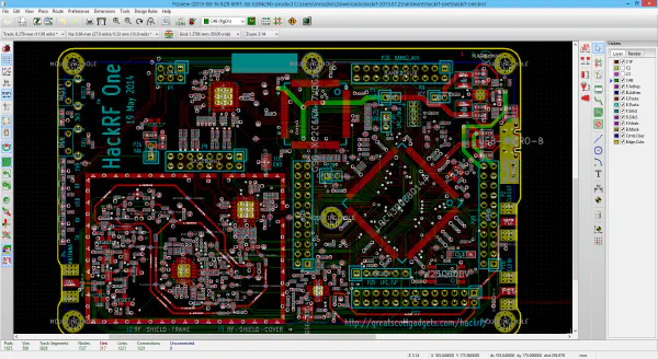
4 Steps to Review the PCB Layout
A comprehensive PCB layout review process covering data collection, placement verification, routing analysis, and …
• 3 min read Electronics Hardware Design
Read more
Showing all posts with tag "Design-Verification"
A comprehensive PCB layout review process covering data collection, placement verification, routing analysis, and …
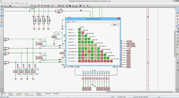
Comprehensive 100-point schematic design checklist covering design rules, components, and verification steps.