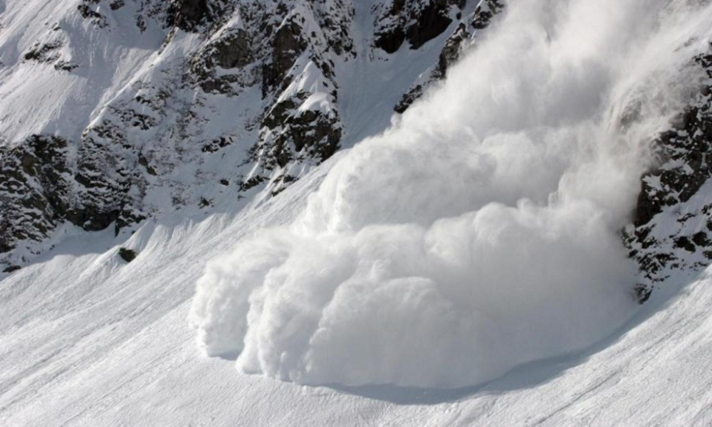
High in the mountains, a delicate balance exists. A single falling stone, no larger than your fist, strikes a snowpack. That impact dislodges a slab. The slab hits another. Within seconds, millions of tons of snow are thundering down the mountainside—an unstoppable cascade triggered by a single event. This is an avalanche, and it’s not just a phenomenon of nature. Deep within the crystalline structure of silicon, under intense electric fields, a similar chain reaction occurs: one electron, accelerated to devastating velocity, strikes an atom and liberates more electrons. Those electrons accelerate, strike more atoms, and within picoseconds, a torrent of current flows through what was moments before an insulator. This is avalanche breakdown, and when you design a diode to harness rather than fear it, you get one of the most versatile components in electronics.
The Physics of Impact Ionization
To understand avalanche breakdown, we need to think about what happens to an electron traveling through silicon under a powerful electric field.
The Acceleration Zone
In a reverse-biased diode, the depletion region acts as an electric highway with no traffic. Majority carriers have been swept away, leaving a nearly empty zone with a steep voltage gradient. When a minority carrier (an electron in a P-type region, or a hole in an N-type region) wanders into this zone, it experiences a massive accelerating force.
The critical insight: If the depletion region is wide enough—typically more than 100 nanometers—the carrier has enough “runway” to accelerate to velocities where its kinetic energy exceeds the band gap energy of silicon (1.1 eV).
The Collision Cascade
When a high-energy electron slams into a silicon atom’s valence electron, it can:
- Transfer enough energy to knock that electron into the conduction band
- Create an electron-hole pair (the process is called impact ionization)
- Both electrons (the original and the newly freed one) continue accelerating
- Both slam into more atoms, creating exponentially increasing carriers
This is the avalanche. Each collision doubles the number of carriers. Within a few nanoseconds, the current multiplies by factors of $10^{3}$ to $10^{6}$.
The Mathematical Model
The multiplication factor ($M$) describes how many carriers emerge for each carrier that enters the depletion region:
$$M = \frac{1}{1 - \left(\frac{V}{V_{BR}}\right)^n}$$Where:
- $V$ = applied reverse voltage
- $V_{BR}$ = breakdown voltage
- $n$ = empirical constant (typically 3-6 for silicon)
As $V$ approaches $V_{BR}$, the denominator approaches zero, and $M$ approaches infinity—the avalanche becomes self-sustaining.
Avalanche vs. Zener: A Tale of Two Breakdowns
Both Zener diodes and avalanche diodes break down when reverse-biased, but the physics and applications are distinct.
| Feature | Zener Breakdown | Avalanche Breakdown |
|---|---|---|
| Mechanism | Quantum tunneling | Impact ionization |
| Voltage Range | < 5V typically | > 6V typically |
| Doping Level | Heavy (thin depletion) | Light (wide depletion) |
| Depletion Width | < 10 nm | > 100 nm |
| Temperature Coefficient | Negative (-2 mV/°C) | Positive (+2 mV/°C) |
| Response Time | ~1 ns | < 100 ps |
| Sharpness | Gradual turn-on | Abrupt turn-on |
| Carrier Type | Direct tunneling (no multiplication) | Exponential multiplication |
The Gray Zone: In the 5V–6V range, both mechanisms occur simultaneously, which is why many “Zener” diodes in this range actually exhibit mixed behavior.
Key Distinction:
- Zener = Electrons tunnel directly through a thin barrier (quantum effect)
- Avalanche = Electrons accelerate and smash into atoms (kinetic effect)
Construction: Engineering the Cascade
An avalanche diode is not accidentally built—it’s precisely engineered to avalanche at a specific voltage without self-destructing.
Doping Profile
Light, uniform doping is critical:
- Too heavy: Depletion region becomes too narrow → Zener tunneling dominates
- Too light: Breakdown voltage becomes too high, energy dissipation becomes unmanageable
- Non-uniform: Creates localized “hot spots” where current concentrates → thermal runaway and failure
Typical doping: $10^{15}$ to $10^{17}$ atoms/cm³ (compare to heavily doped Zener at $10^{18}$ to $10^{20}$ atoms/cm³)
Junction Design
Wide depletion region: The avalanche “runway” must be long enough for carriers to gain sufficient energy. This requires:
- Light doping on at least one side of the junction
- Precise control of the junction depth
- Smooth, defect-free interface (defects create non-uniform fields)
Area considerations:
- Small area: Lower power dissipation, faster response, used in RF and detection
- Large area: Higher power handling, used in surge protection (TVS diodes)
Thermal Management
Because avalanche involves kinetic energy, it generates significant heat. The diode must be designed to spread this heat:
- Die attachment: Soldered or sintered to a thermally conductive substrate
- Package: TO-220, DO-201, or surface-mount packages with exposed thermal pads
- Heat sinking: Essential for continuous operation near breakdown
Applications: Controlled Chaos
1. Transient Voltage Suppression (TVS Diodes)
Purpose: Protect sensitive electronics from voltage spikes (ESD, lightning, inductive kickback)
How it works:
- Normally off (high impedance)
- When a transient exceeds $V_{BR}$, avalanche breakdown occurs instantly (< 1 ns)
- The diode “clamps” the voltage, shunting excess current to ground
- Once the transient passes, the diode returns to blocking state
Performance advantages over other protection:
- Faster than MOVs (Metal Oxide Varistors): < 1 ns vs. ~25 ns
- More robust than gas discharge tubes: No wear-out mechanism
- Lower clamping voltage than Zener: Sharper breakdown knee
Common specifications:
- Standoff voltage ($V_{WM}$): Maximum voltage the TVS can block continuously
- Breakdown voltage ($V_{BR}$): Where avalanche begins (typically 10-20% above $V_{WM}$)
- Clamping voltage ($V_C$): Voltage during surge conduction
- Peak pulse current ($I_{PP}$): Maximum current for 8/20 µs pulse (100A to 10,000A+)
Application example: USB-C port protection
- $V_{WM}$ = 5V (allows normal 5V operation)
- $V_{BR}$ = 6V (tolerate slight overvoltage)
- $V_C$ = 9.5V (clamp transients before damaging 3.3V logic)
2. RF Noise Generation
Purpose: Generate broadband white noise for testing, jamming, or as a signal source
How it works:
- Operate the diode in continuous avalanche breakdown
- The random nature of impact ionization creates shot noise
- Noise is roughly flat (white) from DC to several GHz
- Output power: -140 dBm/Hz to -100 dBm/Hz
Applications:
- Antenna analyzers: Sweep frequency response using broadband noise
- Radio astronomy: Calibration noise source
- Radar testing: Simulate cluttered environments
- Random number generators: True randomness from quantum events
Circuit considerations:
- Series resistor to limit current (typically 1-10 mA)
- Bias near but slightly below $V_{BR}$ for maximum noise output
- Temperature stabilization (breakdown voltage shifts with temperature)
3. Single-Photon Avalanche Diodes (SPADs)
Purpose: Detect individual photons with quantum efficiency approaching 100%
How it works:
- Bias the diode above breakdown voltage (Geiger mode)
- A single photon creates one electron-hole pair
- That pair triggers full avalanche multiplication
- Result: Macroscopic current pulse from a single photon
Performance:
- Photon detection efficiency: 20-70% depending on wavelength
- Dark count rate: 10-10,000 counts/second (thermally generated false triggers)
- Dead time: 10-100 ns (time to “reset” after a detection)
- Timing jitter: 20-100 ps (precision of event timestamp)
Applications:
- LiDAR: Time-of-flight distance measurement (autonomous vehicles)
- Quantum cryptography: Single-photon secure communication
- Medical imaging: PET scanners, fluorescence microscopy
- Astronomy: Detecting faint stars and exoplanet transits
Material selection:
- Silicon: Best for visible light (400-900 nm), low cost
- InGaAs: Near-infrared (900-1700 nm), fiber optic wavelengths
- SiPM arrays: Multiple SPADs in parallel for higher count rates
4. Voltage Reference (High-Voltage)
While Zener diodes dominate low-voltage references (< 6V), avalanche diodes are used for higher voltages.
Advantages:
- Sharper breakdown knee than Zener
- Lower dynamic resistance (better regulation under load changes)
- Positive temperature coefficient (can be compensated by series
Zener)
Application: High-voltage bias supplies for photomultiplier tubes, avalanche photodiodes
Avalanche vs. Schottky: Opposite Ends of the Spectrum
It’s worth contrasting avalanche diodes with Schottky diodes, as they represent opposite design philosophies:
| Feature | Avalanche Diode | Schottky Diode |
|---|---|---|
| Operation | Reverse-bias breakdown | Forward-bias conduction |
| Carriers | Minority → exponential multiplication | Majority only (no multiplication) |
| Speed | Ultra-fast (< 1 ns) | Ultra-fast (< 100 ps) |
| Voltage | High reverse (20V-200V) | Low forward (0.2V-0.4V) |
| Application | Protection, noise, detection | Rectification, RF mixing |
| Junction | P-N (barrier breakdown) | Metal-semiconductor (barrier conduction) |
Ironically, both are “speed demons,” but for opposite reasons: Schottky has no minority carriers to recombine, while avalanche amplifies carriers so rapidly that the response is nearly instantaneous.
Selection Guide: Choosing an Avalanche Diode
For TVS Protection
1. Standoff voltage ($V_{WM}$)
- Must be at least 10% above your maximum operating voltage
- Example: Protecting a 12V rail → choose $V_{WM}$ ≥ 13.2V
2. Clamping voltage ($V_C$)
- Must be below the maximum your circuit can tolerate
- Example: 3.3V logic typically survives 5V → choose $V_C$ < 5V
3. Peak pulse current ($I_{PP}$)
- Must exceed the worst-case surge energy
- Use $ I_{PP} = \frac{E_{surge}}{V_C \times t_{pulse}} $
4. Capacitance
- For high-speed signals (USB 3.0, HDMI, Ethernet), choose < 5 pF
- For power lines, capacitance is less critical
Common parts: SMAJ series, 1.5KE series, P6KE series
For RF Noise
1. Noise figure
- Look for diodes specified for avalanche noise generation
- Typically specialized parts or characterized zeners run in avalanche
2. Operating current
- 1-10 mA is typical for good noise output without excessive heating
3. Frequency range
- Standard avalanche diodes: DC to 1 GHz
- Microwave avalanche diodes: Up to 10+ GHz
For SPADs
1. Photon detection efficiency (PDE)
- Higher is better, but varies with wavelength
- Silicon SPADs peak at ~500 nm (blue-green)
2. Dark count rate (DCR)
- Lower is better for weak signals
- Cooled SPADs can achieve < 10 counts/s
3. Timing jitter
- Critical for time-resolved applications (LiDAR, TCSPC)
- < 50 ps for precision ranging
Specialized vendors: Hamamatsu, SensL, Excelitas, Micro Photon Devices
Common Failure Modes and Precautions
1. Thermal Runaway
Cause: Positive temperature coefficient + localized current → heating → more breakdown → more current
Prevention:
- Ensure uniform doping during manufacturing
- Use heat sinking for continuous operation
- Limit average power dissipation: $P_{avg} = V_{BR} \times I_{avg}$
2. Overvoltage Stress
Cause: Exceeding maximum reverse voltage repeatedly weakens the junction
Prevention:
- Choose $V_{BR}$ with margin above expected transients
- Use series current limiting for RF noise or SPAD applications
3. Surge Energy Overload
Cause: Single transient with energy exceeding the diode’s rating
Example: Lightning strike with 1000A for 100 µs → 100 J
- If TVS diode rated for 10 J, it will fail catastrophically
Prevention:
- Calculate actual surge energy for your application
- Use multiple TVS diodes in parallel if needed
- Add series resistance to dissipate some energy (trade-off: increases clamping voltage)
The Cascade Continues
From the cat’s whisker detector that accidentally created a metal-semiconductor barrier, to Zener diodes that tunnel through quantum barriers, to Schottky diodes that race majority carriers at RF speeds, we arrive at the avalanche diode—a device that takes the most violent breakdown mechanism in semiconductors and turns it into precision protection, quantum detection, and controlled chaos.
The snow slab has become an electronic tool. The cascade, once feared, is now engineered. And every time your phone survives a static shock, every time a quantum cryptography system detects a single photon, every time an RF engineer generates white noise to test an antenna—an avalanche is happening, billions of electrons smashing into silicon atoms in a precisely controlled chain reaction, doing exactly what we designed it to do.
Further Reading
- The Jurassic Schottky: How the Cat’s Whisker Rectified the Radio Age — Historical origins of metal-semiconductor junctions
- The Guardian of Voltage: A Comprehensive Guide to Zener Diodes — Quantum tunneling breakdown
- Schottky Barrier Diodes: The Speed Demons of Modern Electronics — Majority carrier devices
- Application Note: Designing TVS Protection Circuits (coming soon)
- Deep Dive: Single-Photon Avalanche Detector Physics (coming soon)